


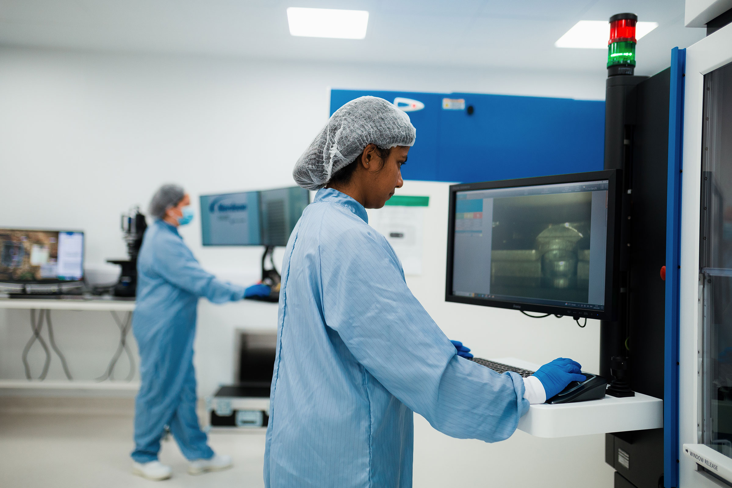
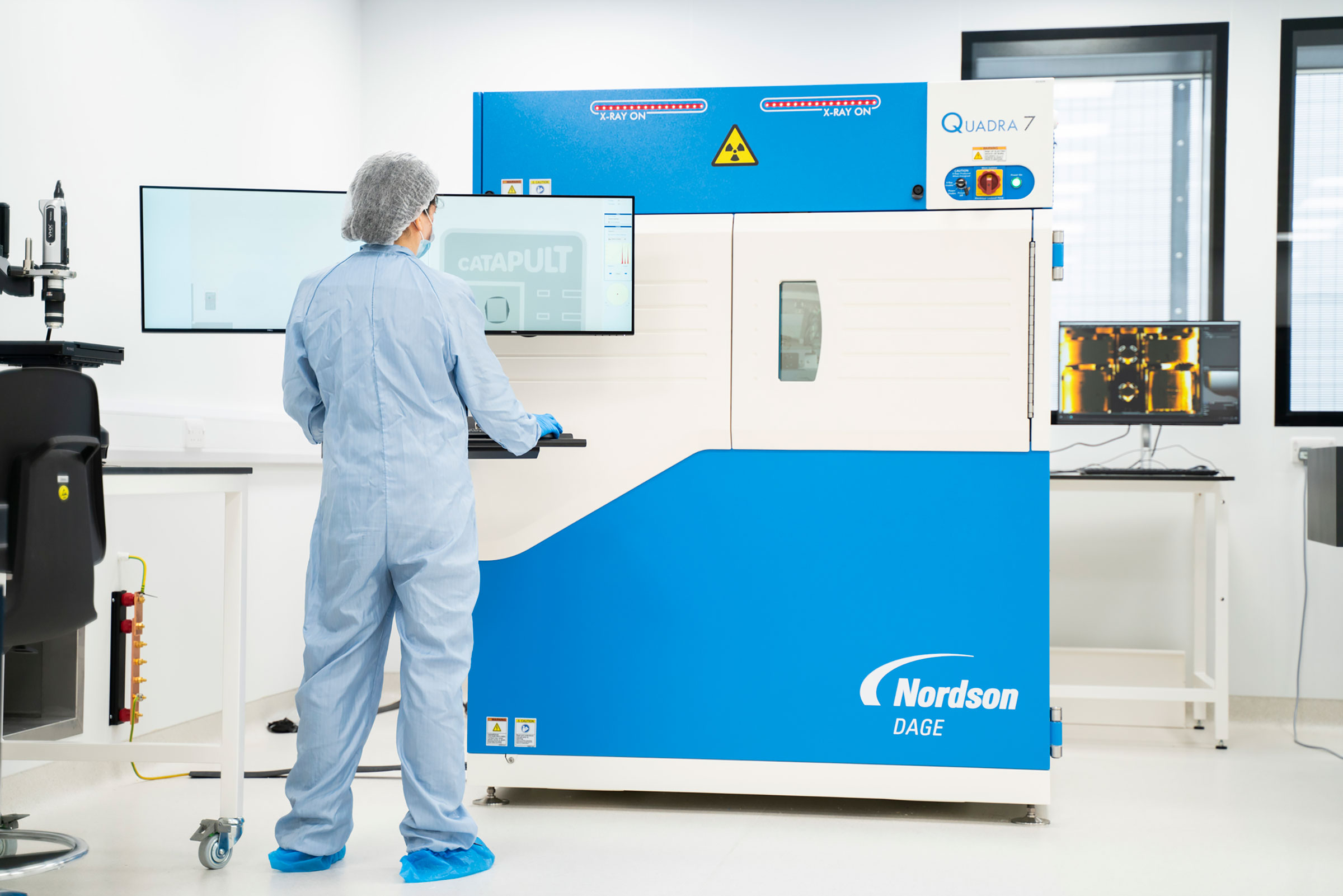
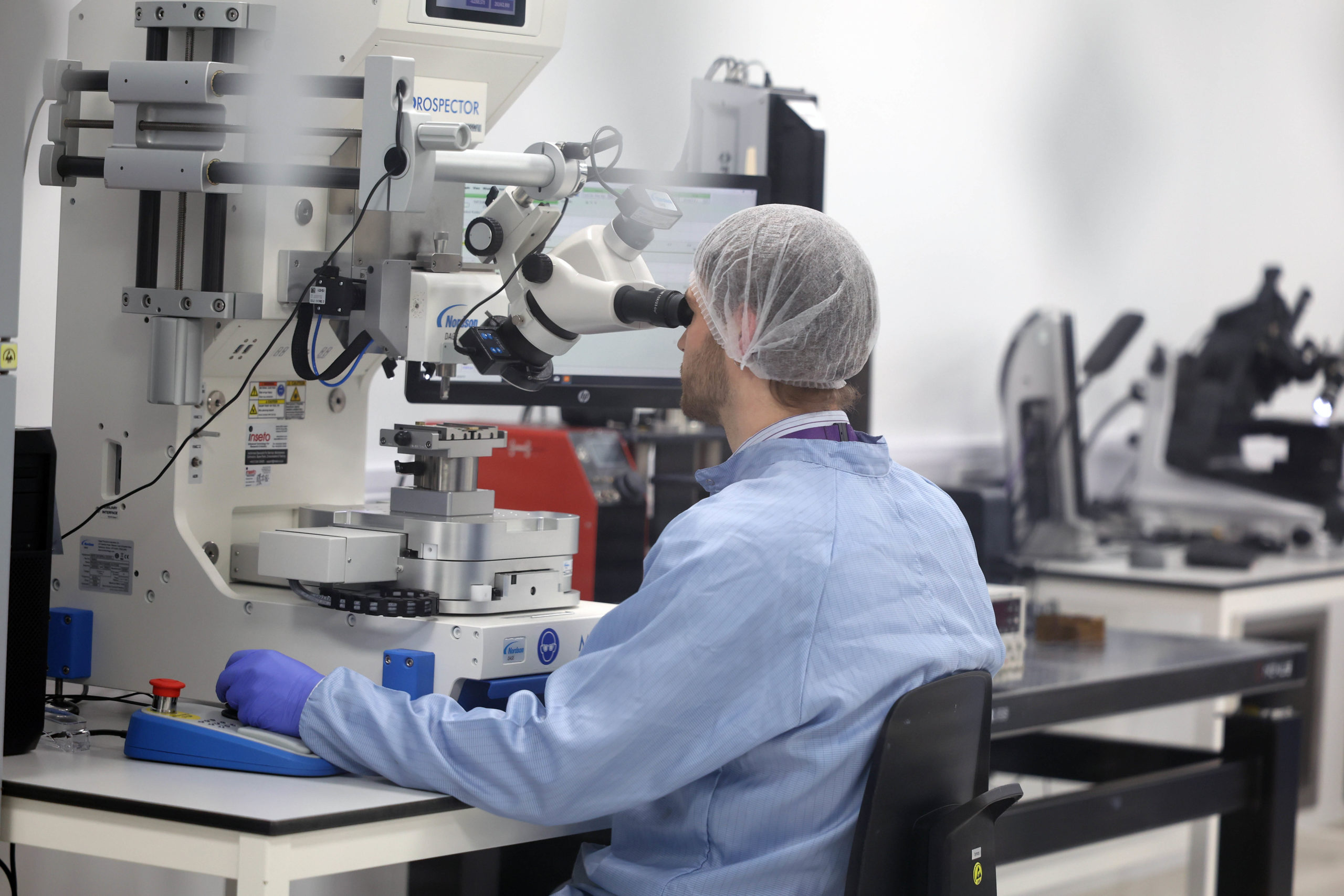
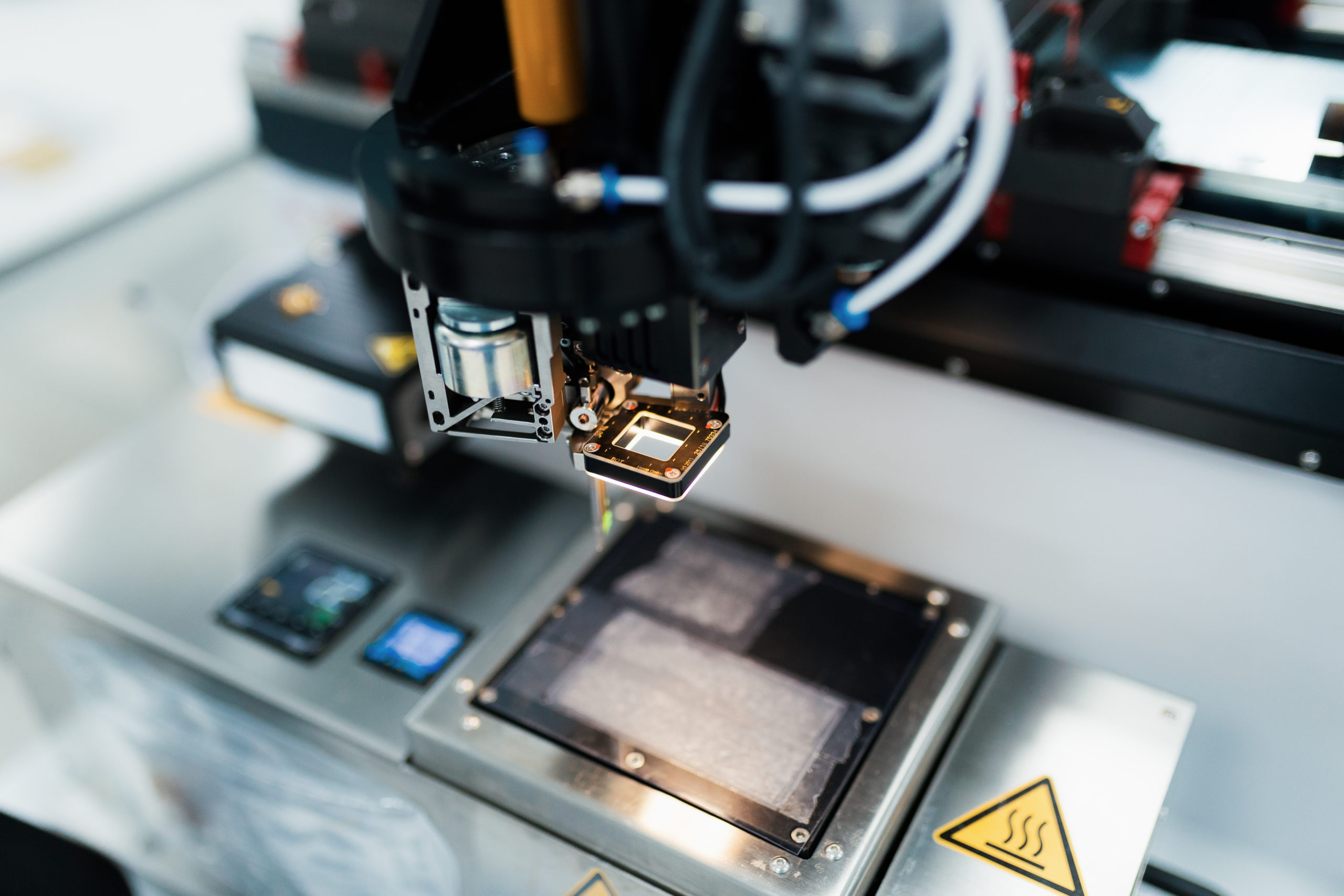
We provide a comprehensive assembly process using the latest tools, techniques and materials that allows you to verify your designs, from proof-of-concept to prototyping.
We provide open access, state-of-the-art assembly equipment.
We have extensive experience of bonding techniques, enabling us to provide novel solutions to shrinking architectures, chip complexity and more dense interconnects.
Thermal Management Evaluation Model: Tackling heat in next-generation electronics
Case studies | Completed Projects | Develop new SME capabilities | Technology acceleration Find out more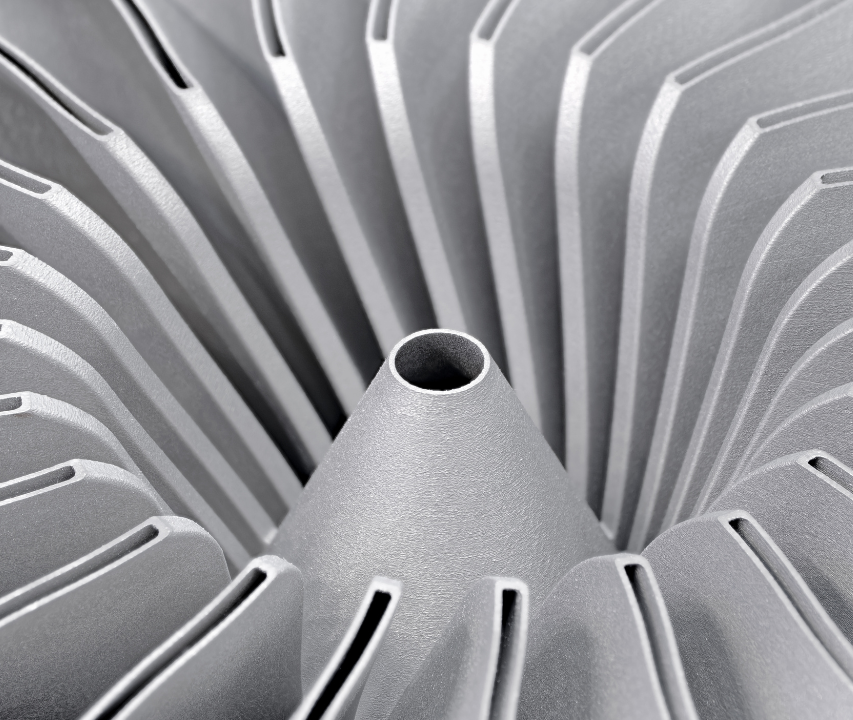
P3EP: Creating a UK supply chain for embedded PCB power electronics systems
Case studies | Completed Projects | First of its kind | Supply chains Find out more
COMPASS: Creating next-generation, energy-efficient sensors for aerospace and communications
Case studies | Completed Projects | Technology acceleration | Job creation/safeguarding Find out more
Playing a key role in the South Wales compound semiconductor cluster
Case studies | Completed Projects | Technology acceleration | Clusters | Supply chains Find out more
Thermal management
Case studies | Completed Projects | Technology acceleration Find out more
High T Hall
Case studies | Completed Projects | Technology acceleration | Supply chains Find out more
Novel power module architecture for cost effective PEMD manufacture (POWERDRIVE)
Live projects | Technology acceleration Find out more
Lignin thermal devices for automotive power electronics
Live projects | Technology acceleration Find out morePower electronics
Our world-leading team of experts has the know-how, experience and track record in developing and commercialising high-performing power electronics devices for automotive, energy and industrial applications.
RF & microwave communications
Our radio frequency and microwave communications experts help optimise the performance and improve the energy efficiency of RF and microwave devices in future telecoms, space, defence and security industries.
Photonics
We are experts in the design, modelling, characterisation and validation of photonics devices, from laser emitters to photonic integrated circuits and quantum hardware.
Advanced packaging
We provide a unique capability in advanced packaging for UK industry. We deliver bespoke solutions to the many complexities associated with compound semiconductor devices.

To learn more about how we can work together, get in touch with a member of our team today.
Contact us
